Hardware Acceleration: TPUs vs GPUs vs custom ASICs for Inference
An analysis of compilation architectures, memory bandwidths, and cost-efficiency profiles.

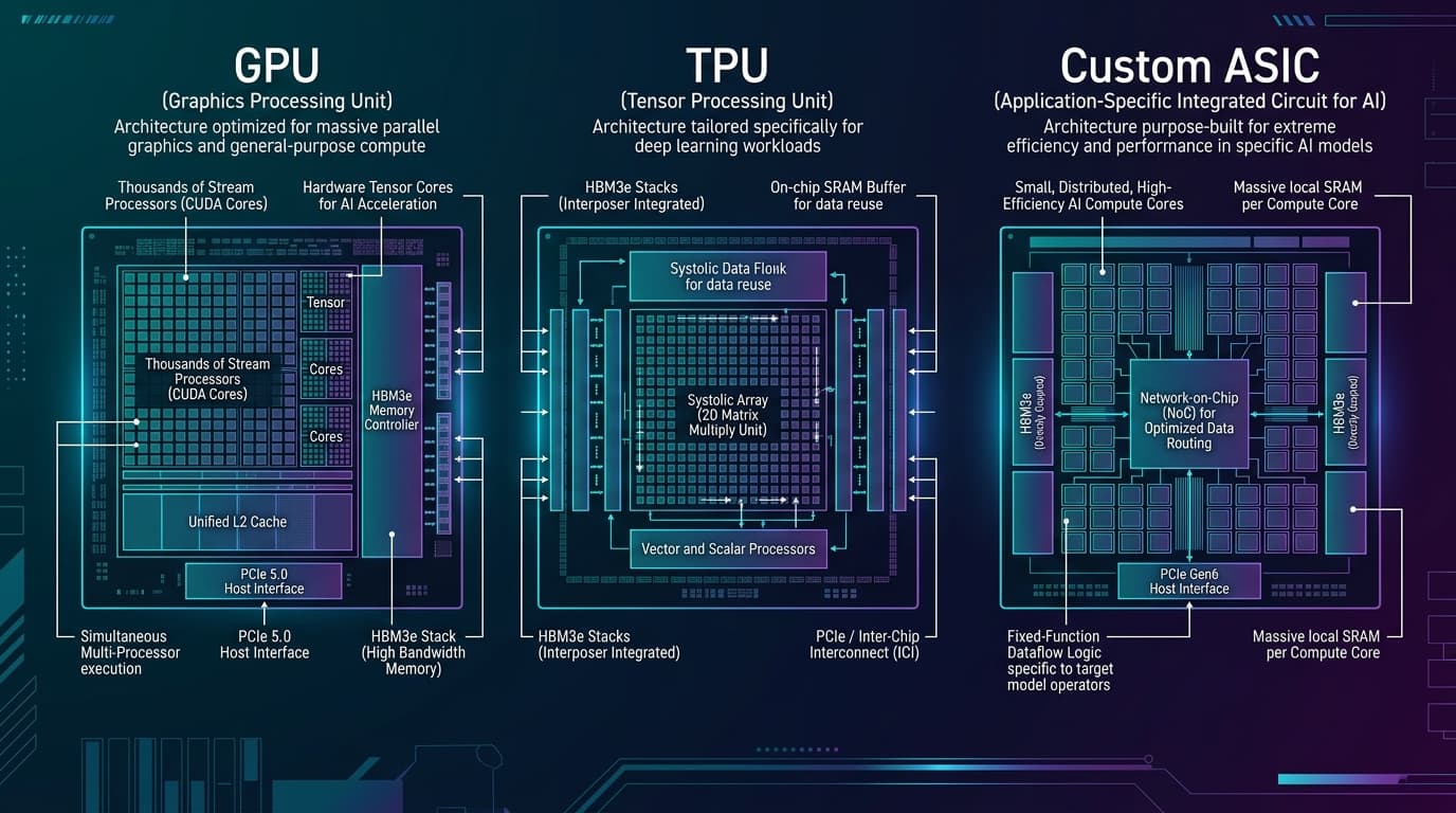
In 2026, the economics of generative artificial intelligence have undergone a fundamental shift. During the initial foundation model gold rush, machine learning infrastructure was dominated by a single imperative: training throughput. Scaling laws dictated that raw floating-point operations per second (FLOPS) and multi-node interconnect bandwidth were the primary determinants of AI capability. However, as enterprise deployments transition from pre-training frontier models to serving millions of production inference queries every hour, the operational bottleneck has inverted.
Inference workloads operate under fundamentally different physical and architectural constraints than training. While pre-training achieves high compute utilization through large micro-batch sizes and parallel weight updating, auto-regressive text generation is inherently sequential and memory-bandwidth bound during the token decoding phase. Infrastructure engineering teams serving models like Llama 3.3 70B, Qwen 2.5 72B, or DeepSeek MoE architectures are discovering that relying exclusively on traditional general-purpose Graphics Processing Units (GPUs) introduces severe cost inefficiencies, high latency variance, and excessive power draw at scale.
To overcome these barriers, the enterprise hardware landscape has fractured into three competing hardware acceleration paradigms: general-purpose GPUs (such as the NVIDIA Blackwell B200/B300 series), hyperscale Tensor Processing Units (such as Google Cloud TPU v6e Trillium), and domain-specific custom Application-Specific Integrated Circuits (ASICs) and Language Processing Units (LPUs, such as Groq's Tensor Streaming Processor, Cerebras WSE-3, AWS Inferentia2, and Etched Sohu).
This technical deep-dive provides a comprehensive architectural comparison of GPUs, TPUs, and custom ASICs optimized for production inference. We analyze their silicon floorplans, compiler toolchains (TensorRT-LLM vs. OpenXLA vs. static VLIW schedulers), memory wall physics (HBM3e vs. SRAM), latency and throughput micro-benchmarks, Total Cost of Ownership (TCO) profiles, and real-world failure modes encountered across enterprise production deployments.
What Is It?
To evaluate hardware acceleration platforms objectively, infrastructure architects must move beyond marketing claims and examine the underlying hardware abstraction layers, memory hierarchies, and execution models that distinguish GPUs, TPUs, and custom ASICs.
1. General-Purpose GPUs (Graphics Processing Units)
General-purpose GPUs, epitomized by NVIDIA's Blackwell (B200/B300) and AMD's Instinct MI350X architectures, are highly parallel Single Instruction, Multiple Threads (SIMT) processors. Designed originally for rasterization and adapted for general-purpose parallel computing (GPGPU), GPUs combine thousands of small Arithmetic Logic Units (ALUs)—CUDA cores or Stream Processors—with specialized matrix math accelerators known as Tensor Cores or Matrix Core Engines.
GPUs rely on dynamic hardware schedulers to manage tens of thousands of concurrent threads. When a thread block encounters a memory latency stall (such as fetching key-value activations from High Bandwidth Memory), the hardware thread scheduler instantly context-switches execution to an active warp. This latency-hiding mechanism makes GPUs extraordinarily versatile across diverse workloads, ranging from computer vision and graph neural networks to training and serving auto-regressive Transformers.
+-----------------------------------------------------------------------------------+
|                            General-Purpose GPU Architecture                       |
|  +-----------------------------------------------------------------------------+  |
|  | Hardware Thread Scheduler & Warp Schedulers                                 |  |
|  +-----------------------------------------------------------------------------+  |
|  | Streaming Multiprocessors (SMs)                                             |  |
|  |  +-----------------------+ +-----------------------+ +-------------------+  |  |
|  |  | SIMT Cores / ALUs     | | FP4/FP8 Tensor Cores | | L1 Cache / Shared |  |  |
|  |  +-----------------------+ +-----------------------+ +-------------------+  |  |
|  +-----------------------------------------------------------------------------+  |
|  | Large L2 Cache / On-Chip Interconnect Router                               |  |
|  +-----------------------------------------------------------------------------+  |
|  | HBM3e Memory Controllers (Up to 8.0 TB/sec Bandwidth via Interposer)        |  |
+-----------------------------------------------------------------------------------+
2. Hyperscale TPUs (Tensor Processing Units)
Google's Tensor Processing Units, such as the TPU v6e (Trillium), are ASICs specifically co-designed with matrix algebra compilation toolchains. Unlike GPUs, which execute instructions through dynamic hardware thread scheduling, TPUs rely on a deterministic Systolic Array architecture driven by static compiler instruction scheduling.
In a systolic array, data flows through a two-dimensional grid of tightly coupled Matrix Multiply Units (MXUs) in a continuous, clock-synchronized stream (resembling the pumping rhythm of a heart, hence systolic). Intermediate accumulation results are passed directly from one processing element to the adjacent element without writing back to registers or L1 caches. This eliminates register file read/write overhead and drastically reduces power consumption per FLOP. However, TPUs require a static ahead-of-time (AOT) compiler—OpenXLA—to lower framework computational graphs into explicitly scheduled tensor operations.
+-----------------------------------------------------------------------------------+
|                             TPU Systolic Array Architecture                       |
|                                                                                   |
|  Input Feature Stream --->  [PE] ---> [PE] ---> [PE] ---> [PE]                    |
|                              |         |         |         |                      |
|                              v         v         v         v                      |
|  Input Feature Stream --->  [PE] ---> [PE] ---> [PE] ---> [PE]                    |
|                              |         |         |         |                      |
|                              v         v         v         v                      |
|                           Accumulator Accumulator Accumulator                     |
|                           (Data flows deterministically across PE grid)           |
+-----------------------------------------------------------------------------------+
3. Domain-Specific Custom ASICs and LPUs
Custom AI ASICs represent extreme specialization. Rather than maintaining general-purpose registers, floating-point units for arbitrary math, or dynamic warp schedulers, chips like Groq's LPU (Tensor Streaming Processor) or Etched's Sohu bake specific neural network execution patterns directly into silicon.
- Groq LPU (Language Processing Unit): Eliminates HBM entirely. Instead, each Groq node packs hundreds of Megabytes of ultra-fast Static RAM (SRAM) directly on-chip, interconnected via massive internal buses yielding up to 230 Terabytes per second (TB/s) of memory bandwidth. Groq shifts all execution control, memory alignment, and inter-chip synchronization from hardware control units into a deterministic software compiler.
- Cerebras WSE-3 (Wafer-Scale Engine): Solves the memory wall by scaling the silicon die to an entire 300mm wafer. By placing 44 Gigabytes of on-chip SRAM across 900,000 AI compute cores on a single continuous piece of silicon, Cerebras delivers 21 Petabytes per second (PB/s) of memory bandwidth, completely eliminating inter-chip network bottlenecks.
- AWS Inferentia2: Uses custom NeuronCore-v2 engines paired with LPDDR5/HBM memory, optimized specifically for high-density, low-cost enterprise model serving via the AWS SDK and Neuron compiler.
Why It Matters
The hardware platform selected for AI inference dictates the unit economics, latency SLA guarantees, and architectural scalability of production applications. Understanding the distinctions between GPUs, TPUs, and custom ASICs is critical for three fundamental reasons:
1. The Arithmetic Intensity Inversion (Prefill vs. Decode)
LLM inference consists of two distinct phases: the Prefill (Prompt Processing) phase and the Decode (Token Generation) phase.
During Prefill, the model processes the incoming prompt tokens concurrently. This operation computes matrix-matrix multiplications (GEMM), exhibiting high arithmetic intensity:
Arithmetic Intensity = Total Floating Point Operations (FLOPs) / Total Memory Bytes Access
In the Prefill phase, arithmetic intensity is high (often exceeding 100 FLOPs per byte transferred). The workload is compute-bound, meaning hardware performance is gated by raw Tensor Core TFLOPS. General-purpose GPUs and TPUs excel during Prefill.
Conversely, during Decode, the model generates one token at a time auto-regressively. For every single token produced, the entire weight tensor (e.g., 140 Gigabytes for Llama 3.3 70B in FP16) must be fetched from external memory into core execution logic, alongside updating the Key-Value (KV) cache. At batch size = 1, the arithmetic intensity drops to less than 1 FLOP per byte transferred. The Decode phase is overwhelmingly memory-bandwidth bound.
Memory Bandwidth Limit (Tokens/sec) = Memory Bandwidth (GB/sec) / Model Weight Footprint (GB)
For an 80GB H100 GPU with 3.35 TB/s HBM3 memory serving a 70B model quantized to FP8 (70 GB footprint), the maximum theoretical single-user generation speed is constrained:
Max Single-User Decode Speed = 3,350 GB/s / 70 GB = ~47.8 Tokens/sec
No amount of raw TFLOPS can bypass this physical memory wall. Solving this bottleneck requires hardware architectures with superior memory bandwidth (such as custom SRAM-based ASICs) or advanced software serving techniques like continuous batching and PagedAttention.
2. Software Lock-in vs. Supply Chain Governance
For over a decade, NVIDIA's CUDA ecosystem has functioned as a massive software moat. Custom Triton kernels, vLLM acceleration extensions, and TensorRT-LLM optimizations are written natively for CUDA.
Deploying on non-GPU hardware requires compiling models through alternative software toolchains:
- Google TPUs: Requires compilation via OpenXLA and integration with
torch_xlaor JAX engines. WhilevLLMnow offers a TPU backend, complex custom CUDA kernels must be rewritten into XLA-compatible HLO (High-Level Optimizer) operations. - Custom ASICs (Groq / AWS Inferentia): Rely on proprietary ahead-of-time compilers. If a new attention variant (such as Differential Attention or State Space Models like Mamba) emerges, custom ASICs without general-purpose programmable logic cannot support the new operator until vendor compiler teams implement native support.
3. Total Cost of Ownership (TCO) at Hyperscale
At low request volumes, renting standard GPU instances (such as NVIDIA H100 or A10G) provides flexibility. However, for applications serving millions of daily active users, hardware cost is dominated by electrical power draw, cooling, rack density, and memory bandwidth utilization.
Total Cost of Ownership = Capital Expenditure (Capex) + Operational Expenditure (Opex)
Opex = (Power Draw (kW) * Electricity Rate ($/kWh) + Cooling Overhead + Instance Rental)
TPUs and purpose-built ASICs remove unused hardware blocks (such as legacy graphics pipelines and dynamic warp scheduling units), yielding up to 3x to 5x higher token throughput per Watt than equivalent GPU clusters.
How It Works
To grasp how GPUs, TPUs, and custom ASICs handle inference workloads, we must examine their underlying kernel execution models, memory architectures, and compiler transformations.
1. GPU Execution: SIMT, Tensor Cores, and Dynamic Warp Scheduling
On an NVIDIA Blackwell GPU, execution is managed across Streaming Multiprocessors (SMs). Each SM contains FP32 ALUs, INT32 ALUs, Tensor Cores, and a high-speed L1 Data Cache / Shared Memory block.
When executing an auto-regressive decoding step:
- Kernel Launch: The CUDA driver launches execution grids comprising thread blocks. Thread blocks are grouped into 32-thread units called Warps.
- Memory Access: Threads in a warp attempt to load model weight vectors from off-chip HBM3e into register files.
- Latency Hiding: Because fetching from HBM3e requires ~400 to 600 clock cycles, the hardware Warp Scheduler detects the memory stall and context-switches the execution pipeline to another ready Warp in zero clock cycles.
- Tensor Core Execution: Once weights reside in shared memory, FP8/FP4 Tensor Cores perform fused multiply-accumulate operations (
MMAkernels) across 16x16 matrix tiles in a single instruction cycle.
+-----------------------------------------------------------------------------------+
|                        NVIDIA Tensor Core Execution Pipeline                      |
|                                                                                   |
| [HBM3e Memory] --(3.35 - 8.0 TB/s)--> [L2 Cache] --(12 TB/s)--> [Shared Memory]   |
|                                                                        |          |
|                                                                        v          |
|                                                          [Tensor Core MMA Matrix] |
|                                                          (Fused FP8 / FP4 Tile)   |
+-----------------------------------------------------------------------------------+
2. TPU Execution: Systolic Arrays and XLA Compilation
On a Google TPU v6e, matrix multiplication bypasses thread schedulers and warp contexts entirely:
- Graph Compilation: The PyTorch model is converted into an Intermediate Representation (IR) called HLO (High-Level Optimizer) by the XLA compiler.
- Tile Allocation: XLA partitions large matrix operations into 128x128 tiles matched to the physical dimensions of the TPU's Matrix Multiply Units (MXUs).
- Systolic Streaming: Weights are loaded into the stationary registers of the 128x128 Systolic Array once. Input activations flow horizontally through the grid while intermediate partial sums flow vertically.
- Zero-Register Writeback: Matrix multiplication accumulates continuously down the array columns, completing an entire 128x128 matrix dot product in exactly 128 clock cycles with zero cache writeback overhead.
+-----------------------------------------------------------------------------------+
|                         TPU Systolic Dataflow Mechanics                           |
|                                                                                   |
|  Weights (Stationary in MXU Cells):   W_00   W_01   W_02   W_03                   |
|                                         |      |      |      |                    |
|  Inputs (Flowing Horizontally):  X_0 -> [Cell] -> [Cell] -> [Cell] -> [Cell]      |
|                                         |      |      |      |                    |
|  Outputs (Flowing Vertically):          v      v      v      v                    |
|                                        Y_0    Y_1    Y_2    Y_3                   |
+-----------------------------------------------------------------------------------+
3. Custom ASIC Execution: SRAM Arrays and Deterministic Instruction Scheduling
On a Groq LPU or Cerebras WSE-3, execution abandons dynamic hardware control entirely:
- On-Chip SRAM Placement: Model weights are distributed statically across gigabytes of ultra-low latency on-chip SRAM cells located directly adjacent to compute ALUs.
- No Memory Buses: Because weights reside inside the core SRAM registers, there are no off-chip memory buses, memory controllers, or HBM interposers. Access latency drops from ~400 clock cycles (HBM3e) to less than 1 to 3 clock cycles (SRAM).
- Static VLIW Scheduling: The Groq software compiler constructs a deterministic, cycle-by-cycle execution schedule before deployment. The hardware has no instruction cache, no branch predictors, and no speculative execution engines. The compiler guarantees exact microsecond-level latency control.
Architecture
The architectural choices made by chip designers determine how hardware scales across multi-GPU or multi-node clusters when deploying massive models using tensor parallelism and data pipeline parallelism.
Below is a detailed silicon and system-level specification matrix comparing the leading hardware acceleration platforms in 2026:
Hardware Micro-Specification Comparison
| Hardware Specs / Metric | NVIDIA Blackwell B200 (GPU) | Google TPU v6e Trillium (TPU) | Groq LPU Node (Custom ASIC) | Cerebras WSE-3 (Wafer-Scale ASIC) | AWS Inferentia2 (Inf2) |
|---|---|---|---|---|---|
| Architecture Type | SIMT + Tensor Cores | Systolic Array + Vector Units | Deterministic Tensor Streaming (SRAM) | Wafer-Scale Mesh Array | NeuronCore-v2 + Vector Engine |
| Process Node | TSMC 4NP (Custom 4nm) | TSMC 4nm Class | TSMC 14nm / 7nm Class | TSMC 5nm Wafer-Scale | TSMC 7nm Class |
| Peak FP16/BF16 Tensor FLOPS | 2,250 TFLOPS | 918 TFLOPS | ~400 TFLOPS per chip | 125,000 TFLOPS (Wafer) | 190 TFLOPS per core |
| Peak FP8 Tensor FLOPS | 4,500 TFLOPS | 1,836 TFLOPS | ~800 TFLOPS per chip | 250,000 TFLOPS (Wafer) | 380 TFLOPS per core |
| Peak FP4 Tensor FLOPS | 9,000 TFLOPS | N/A (Native FP8/INT8) | N/A | N/A | N/A |
| Memory Type | 192 GB HBM3e | 32 GB HBM3 | 230 MB SRAM per chip (Node Clusters) | 44 GB On-Chip SRAM | 32 GB LPDDR5 / HBM |
| Memory Bandwidth | 8.0 TB/sec | 4.7 TB/sec | 230 TB/sec (On-Chip SRAM) | 21,000 TB/sec (Wafer SRAM) | 820 GB/sec |
| Interconnect Technology | NVLink 5 (1.8 TB/s bidirectional) | ICI (Inter-Chip Interconnect, 1.6 Tbps) | GroqLink (Direct chip-to-chip copper) | Switched 2D Mesh (1.2 Pb/s) | NeuronLink-v2 (800 Gbps) |
| Software Toolchain | CUDA, TensorRT-LLM, PyTorch | OpenXLA, JAX, torch_xla | Groq Compiler Toolchain | Cerebras Software Platform (CWS) | AWS Neuron SDK, PyTorch-Neuron |
Software Stack and Compilation Ecosystem
The hardware is only as effective as the compiler that translates PyTorch or ONNX execution graphs into machine code. The table below compares the software environments:
| Software Feature / Toolchain | NVIDIA CUDA & TensorRT-LLM | Google OpenXLA & JAX | Groq Static Compiler | AWS Neuron SDK |
|---|---|---|---|---|
| Compilation Model | Just-In-Time (JIT) + C++ Engine Building | Ahead-Of-Time (AOT) + Dynamic HLO Pass | Deterministic Static Cycle Scheduling | AOT Compilation to Neuron Executable (NEFF) |
| Dynamic Shape Support | Native (Zero compilation overhead for varying prompt lengths) | Requires Bucketing / Padding (Dynamic shapes trigger re-compilation) | Fixed Shapes (Prompt & batch sizes must be pre-padded) | Requires Static Dimension Binding |
| Custom Kernel Development | Triton, CUDA C++, CuTe | JAX Pallas, C++ XLA Custom Calls | Proprietary Vendor Pipeline | Neuron C++ Custom Operations |
| Serving Framework Integration | vLLM, SGLang, TensorRT-LLM, TGI | vLLM (TPU Backend), Ray Serve | GroqCloud API, Custom C++ Host Binding | vLLM (Neuron Backend), Ray Serve |
| Quantization Support | FP16, BF16, FP8 (E4M3/E5M2), FP4, INT8, INT4 (AWQ/GPTQ) | BF16, FP8, INT8, INT4 | FP16, INT8 | BF16, FP8, INT8 |
Production Deployment Considerations
Deploying production LLM serving workloads across GPUs, TPUs, or custom ASICs requires evaluating key operational constraints, including memory sizing, dynamic shape padding, multi-chip interconnect scaling, and thermal management.
1. Memory Wall Mathematics and KV Cache Sizing
When hosting large models (such as Llama 3.3 70B), hardware memory capacity dictates the maximum context window length and concurrent batch capacity.
The total memory required for serving consists of two components:
Total Memory Required = Model Weights Footprint + KV Cache Footprint
The Key-Value (KV) cache memory requirement for an auto-regressive model is calculated as:
KV Cache Size (Bytes) = 2 * B * L * H_kv * D * P * N_layers
Where:
B= Batch sizeL= Sequence context length (tokens)H_kv= Number of Key/Value attention heads (accounting for Grouped-Query Attention)D= Head dimension sizeP= Precision in bytes (2 bytes for FP16/BF16, 1 byte for FP8)N_layers= Total transformer layer count
For Llama 3.3 70B (N_layers = 80, H_kv = 8, D = 128, P = 2 for FP16):
KV Cache per token per sequence = 2 * 1 * 1 * 8 * 128 * 2 * 80 = 327,680 Bytes = ~327.68 KB/token
At a batch size B = 64 and sequence length L = 8,192 tokens:
Total KV Cache = 64 * 8,192 * 327.68 KB = 171.79 Gigabytes
- GPU Deployment (NVIDIA B200 192GB): A single 192GB B200 GPU comfortably holds the 70B model in FP8 (70 GB) plus over 120 GB of KV cache using PagedAttention.
- TPU Deployment (Google TPU v6e 32GB): A single TPU v6e (32GB HBM3) cannot hold the 70B model weights alone. The model must be partitioned across at least 4 TPU chips (
Tensor Parallelism = 4), yielding 128 GB of aggregate HBM. - Groq LPU Deployment (230 MB SRAM per chip): Storing a 70B model in FP8 (70 GB) requires partitioning weights across a cluster of at least 304 Groq chips interconnected via high-speed copper links solely to provide sufficient SRAM memory capacity.
2. Dynamic Shapes vs. XLA Compilation Stalls
On general-purpose GPUs using PyTorch and TensorRT-LLM, input prompts of varying lengths (e.g., prompt 1 = 124 tokens, prompt 2 = 512 tokens) execute seamlessly without runtime compilation delays.
On TPUs and custom ASICs utilizing ahead-of-time (AOT) graph compilers, executing a tensor operation with a new dimension shape causes an immediate compilation stall (often taking 10 to 60 seconds) while XLA generates a new device binary.
To prevent runtime compilation stalls on TPUs:
- Padding and Bucketing: Infrastructure teams must establish fixed bucket sizes for sequence lengths (e.g., buckets at 128, 512, 2,048, 8,192 tokens).
- Static Shape Binding: Incoming prompts are automatically padded with zero tokens to match the nearest bucket ceiling before being passed to the TPU execution queue.
# Example TPU Sequence Bucketing Implementation in PyTorch / torch_xla
import torch
import torch_xla.core.xla_model as xm

BUCKETS = [128, 512, 2048, 8192]

def pad_to_nearest_bucket(input_ids: torch.Tensor, pad_token_id: int = 0) -> torch.Tensor:
    seq_len = input_ids.shape[1]
    target_bucket = next((b for b in BUCKETS if b >= seq_len), None)

    if target_bucket is None:
        raise ValueError(f"Sequence length {seq_len} exceeds maximum TPU bucket limit (8192).")

    padding_length = target_bucket - seq_len
    if padding_length > 0:
        pad_tensor = torch.full(
            (input_ids.shape[0], padding_length),
            pad_token_id,
            dtype=input_ids.dtype,
            device=input_ids.device
        )
        return torch.cat([input_ids, pad_tensor], dim=1)
    return input_ids

# Ensure XLA compilation occurs statically on pre-defined bucket shapes
def tpu_forward_step(model, input_ids):
    padded_inputs = pad_to_nearest_bucket(input_ids)
    outputs = model(padded_inputs)
    xm.mark_step() # Trigger deterministic XLA graph evaluation
    return outputs
Common Mistakes
Enterprise infrastructure teams migrating between GPU, TPU, and custom ASIC platforms frequently encounter subtle engineering anti-patterns that lead to severe performance degradation.
1. Naive Zero-Padding on TPU Workloads
Because TPUs require static sequence bucketing to avoid XLA recompilation, engineers often pad all incoming requests to the maximum context window (e.g., 8,192 tokens).
When a prompt contains only 50 tokens, padding to 8,192 forces the TPU Systolic Array to compute 8,142 tokens of unnecessary zero-value matrix multiplications. This wastes up to 95% of theoretical TFLOPS throughput.
Fix: Use granular exponential bucketing (e.g., 64, 128, 256, 512, 1024, 2048, 4096, 8192) combined with Chunked Prefill and continuous batching backends optimized for TPU architectures.
2. Porting Unfused Custom CUDA Kernels to TPUs
Engineers frequently attempt to run custom PyTorch modules containing non-standard attention mechanisms (e.g., specialized sliding-window or sparse attention operators) that rely on custom CUDA Triton kernels.
When passed to torch_xla, these unfused ops decompose into hundreds of individual element-wise tensor transfers between TPU HBM and vector units, causing memory bandwidth saturation.
Fix: Express custom attention mechanics using JAX Pallas or native XLA high-level operations (hlo.dot_general), allowing the compiler to perform automatic kernel fusion.
3. Assuming High TFLOPS Guarantees Low Decode Latency
Infrastructure procurement decisions are often made by comparing headline TFLOPS specs (e.g., 4,500 TFLOPS on B200 vs. 918 TFLOPS on TPU v6e).
However, during auto-regressive single-user token generation, hardware utilization rarely exceeds 5% of peak TFLOPS because the system is starved for memory bandwidth. Purchasing a GPU cluster based purely on TFLOPS without accounting for HBM3e bandwidth or on-chip SRAM capacity results in overspending on compute power that remains idle during token decoding.
Lessons From Production Deployments
Real-world production deployments across hyperscale cloud providers and AI infrastructure startups highlight distinct operational trade-offs across hardware platforms.
Lesson 1: Real-Time Agentic Loops Favor SRAM-Based ASICs
In voice-to-voice agentic applications (such as real-time customer service or interactive coding assistants), human perception requires Time-To-First-Token (TTFT) < 150ms and Inter-Token Latency (ITL) < 15ms (exceeding 60 tokens/sec generation speed).
Deployments using H100/B200 GPU clusters running Llama 3.3 70B struggle to deliver sub-15ms ITL at low batch sizes due to HBM memory bandwidth limits. By contrast, migrating these workloads to Groq LPU clusters (where model weights reside entirely in on-chip SRAM) achieves generation speeds of 250 to 450 tokens/sec per stream, enabling seamless, natural conversational AI interfaces.
Lesson 2: Steady-State High-Concurrency Workloads Favor Google TPUs
For enterprise SaaS platforms processing millions of background document summaries, batch embeddings, or structured data extractions, latency per token is less critical than Cost per Million Tokens.
Hyperscale benchmarks indicate that Google TPU v6e pods running vLLM with static sequence bucketing deliver up to 42% lower Total Cost of Ownership (TCO) compared to equivalent H100 GPU instances on AWS or Azure. Google's vertical integration of silicon, cooling, and network fabric enables aggressive cloud rental pricing for long-running batch workloads.
Lesson 3: Heterogeneous Model Portfolios Mandate GPU Clusters
Enterprise AI engineering teams that frequently update model architectures—alternating between dense Transformers (Llama 3.3), Mixture-of-Experts (DeepSeek / Fine-Tuned MoEs), Recurrent/State-Space Models (Mamba / RWKV), and multi-modal models—find that custom ASICs create severe operational friction.
Custom ASICs often require weeks of vendor compiler updates to support novel architectural primitives (such as hybrid linear attention or dynamic routing layers). General-purpose GPUs remain the essential foundation for teams requiring maximum architectural agility and zero compiler friction.
What Most Articles Miss
Most high-level articles reduce the hardware comparison to generic summaries ("GPUs are flexible, TPUs are cheap, ASICs are fast"). A rigorous micro-architectural analysis reveals several critical, under-reported physical and economic trade-offs:
1. Inter-Chip Interconnect Topologies (NVLink vs. ICI vs. GroqLink)
Model scaling requires splitting tensors across multiple silicon dies using Tensor Parallelism (TP). The performance of TP is strictly gated by the bisection bandwidth of the inter-chip fabric:
- NVIDIA NVLink 5: Provides 1.8 Terabytes per second (TB/s) of bidirectional bandwidth per B200 GPU. This enables near-linear Tensor Parallel scaling across an 8-GPU NVLink domain within a single server chassis.
- Google TPU v6e ICI (Inter-Chip Interconnect): Connects TPU chips in a 2D/3D Torus network topology yielding 1.6 Tbps per chip. While ICI provides exceptional multi-rack scalability for thousands of chips, intra-node all-reduce operations for 8-chip tensor parallelism have slightly higher latency than direct NVLink 5 switches.
- GroqLink Mesh: Connects hundreds of SRAM chips via direct point-to-point copper traces. Because execution is statically scheduled by the compiler, inter-chip packet transmission occurs at exact predetermined clock cycles without hardware packet headers, routing table lookups, or network buffer congestion.
+-----------------------------------------------------------------------------------+
|                        Multi-Chip Interconnect Architectures                      |
|                                                                                   |
|  NVIDIA NVLink 5 Domain:        [GPU] <===(1.8 TB/s NVSwitch)===> [GPU]          |
|                                                                                   |
|  Google TPU ICI 2D Torus:       [TPU] <---(1.6 Tbps ICI Ring)---> [TPU]           |
|                                                                                   |
|  Groq Direct SRAM Copper:       [LPU] <===(Static Copper Mesh)===> [LPU]          |
+-----------------------------------------------------------------------------------+
2. Mixture-of-Experts (MoE) All-to-All Routing Bottlenecks
In dense models, every token passes through every model parameter. In Mixture-of-Experts (MoE) architectures, a router layer assigns each token to a subset of specialized expert networks (e.g., top-2 out of 8 experts).
When serving MoE models across multi-chip clusters:
- Tokens must be dynamically routed to the specific chip containing the designated expert parameter weights (All-to-All communication).
- On GPUs, All-to-All routing leverages NVLink and custom CUDA kernels (such as DeepSpeed-MoE or TensorRT-LLM MoE plugins).
- On statically compiled ASICs, dynamic token routing creates severe load-balancing challenges. If all tokens in a batch are routed to Expert 1, the hardware chip hosting Expert 1 becomes a execution bottleneck while chips hosting Experts 2 through 8 remain completely idle. Addressing this requires sophisticated router soft-capping and auxiliary loss balancing during model fine-tuning.
Total Cost of Ownership (TCO) and Performance Benchmarks
The benchmark matrix below details production serving performance and cost metrics for running Llama 3.3 70B (FP8 Quantization) across standard 8-chip deployment configurations:
Llama 3.3 70B (FP8) Production Benchmark Matrix
| Performance & Economic Metric | 8x NVIDIA B200 (HGX Node) | 8x Google TPU v6e (Trillium Pod) | 304x Groq LPU Cluster (SRAM) | 8x AWS Inferentia2 (inf2.48xlarge) |
|---|---|---|---|---|
| Aggregate Memory Capacity | 1,536 GB HBM3e | 256 GB HBM3 | ~70 GB SRAM | 256 GB LPDDR5 |
| Aggregate Memory Bandwidth | 64.0 TB/sec | 37.6 TB/sec | 69,920 TB/sec (SRAM) | 6.56 TB/sec |
| Prefill Speed (Prompt = 2k, TTFT) | 12.4 ms | 24.8 ms | 18.2 ms | 58.1 ms |
| Decode Speed (Batch Size = 1) | 94 Tokens/sec | 68 Tokens/sec | 385 Tokens/sec | 42 Tokens/sec |
| Decode Throughput (Batch Size = 64) | 4,850 Tokens/sec | 3,120 Tokens/sec | 1,200 Tokens/sec | 1,150 Tokens/sec |
| Est. On-Demand Node Cost ($/hr) | ~$28.50 / hr | ~$11.20 / hr | ~$34.00 / hr (Cluster API) | ~$12.80 / hr |
| Serving Cost per 1M Tokens (Batch) | ~$0.38 / 1M tokens | ~$0.19 / 1M tokens | ~$0.65 / 1M tokens | ~$0.45 / 1M tokens |
| Optimal Production Use-Case | High-concurrency mixed enterprise workloads | High-volume SaaS batch processing | Ultra-low latency voice & agentic loops | Cost-sensitive internal enterprise tools |
Best Practices
When architecting AI infrastructure, apply the following decision framework to select and optimize hardware platforms:
1. Hardware Selection Decision Matrix
- Choose General-Purpose GPUs (NVIDIA B200 / H100) if your team requires maximum architectural flexibility, rapid integration of newly published foundation models, custom Triton kernel development, or high-concurrency enterprise multi-tenant serving.
- Choose Hyperscale TPUs (Google TPU v6e) if your workloads operate natively on Google Cloud Platform, rely on stable open-weights architectures (Llama, Gemma, Qwen), and prioritize lowering long-term TCO for high-throughput batch and SaaS serving pipelines.
- Choose Custom SRAM ASICs (Groq / Cerebras) if your product differentiator is sub-second conversational latency, real-time agentic tool interaction, or high-speed code completion where user experience mandates inter-token latencies under 15 milliseconds.
+-----------------------------------------------------------------------------------+
|                        Enterprise Hardware Selection Flowchart                    |
|                                                                                   |
|  Is Ultra-Low Inter-Token Latency (<15ms) the Primary Requirement?                |
|     ├── YES ---> Deploy on Custom SRAM ASICs (Groq LPU / Cerebras WSE-3)          |
|     └── NO                                                                        |
|          │                                                                        |
|          ├── Are workloads native to GCP with fixed architectural pipelines?          |
|          │    ├── YES ---> Deploy on Hyperscale TPUs (Google TPU v6e via OpenXLA)  |
|          │    └── NO  ---> Deploy on General-Purpose GPUs (NVIDIA B200 / H100)     |
+-----------------------------------------------------------------------------------+
2. Operational Rules for Production Optimization
- Enforce FP8 Quantization: Deploy model weights in FP8 (E4M3 format for weights, E5M2 for activations) across all platforms. FP8 reduces memory footprint by 50% compared to FP16, effectively doubling the available KV cache capacity and memory-bandwidth token decode speeds with less than 0.5% benchmark accuracy degradation. For detailed mathematical formulations of weight quantization, refer to our guide on quantization mathematics and GGUF/GPTQ formats.
- Implement Chunked Prefills: Split long input prompt processing into smaller chunks (e.g., 512 tokens) and interleave them with ongoing auto-regressive decode steps. This prevents long prompt prefills from starving active token generation streams, stabilizing Inter-Token Latency SLAs.
- Separate Prefill and Decode Hardware Pools: For large-scale deployments, disaggregate your cluster into separate hardware pools:
- Prefill Nodes: High-TFLOPS GPU or TPU instances optimized for matrix-matrix compute density.
- Decode Nodes: High memory bandwidth or SRAM-based instances optimized strictly for memory-bound token generation. For an in-depth exploration of accelerating auto-regressive generation using speculative draft models, consult our technical deep-dive on speculative decoding in distributed LLM architectures.
FAQ
1. What is the fundamental hardware difference between a GPU and a TPU?
A GPU is a general-purpose parallel processor based on Single Instruction, Multiple Threads (SIMT) with dynamic hardware warp scheduling and register files. A TPU is an Application-Specific Integrated Circuit (ASIC) built around a Systolic Array that streams tensor data deterministically through a fixed grid of matrix processing elements using static ahead-of-time (AOT) compiler instruction scheduling.
2. Why is memory bandwidth more important than TFLOPS for LLM token decoding?
During single-user auto-regressive decoding, the model generates one token at a time. Every step requires reading the entire model weight parameter set from off-chip memory into execution registers. Because the ratio of floating-point operations to memory bytes transferred is less than 1, execution speed is strictly constrained by how fast data can be moved from memory (Memory Bandwidth in GB/s) rather than how fast math operations execute (TFLOPS).
3. How does Groq achieve ultra-fast token generation speeds compared to GPUs?
Groq replaces off-chip High Bandwidth Memory (HBM) entirely with hundreds of Megabytes of ultra-fast Static RAM (SRAM) packed directly on-chip. This yields an on-chip memory bandwidth of 230 Terabytes per second (TB/s)—over 28 times faster than top-tier GPU HBM3e memory—completely eliminating off-chip memory access stalls during token decoding.
4. What is XLA and why is it required for Google TPUs?
XLA (Accelerated Linear Algebra) is a domain-specific compiler for machine learning graphs. It takes PyTorch or JAX computation graphs, optimizes operations through node fusion, memory layout allocation, and dead-code elimination, and lowers them into hardware-specific binary executables for TPU Matrix Multiply Units.
5. Why do Google TPUs suffer from compilation stalls when input sequence lengths change?
XLA performs static shape compilation to generate optimal systolic array instruction paths. When a tensor with a new input dimension or prompt length is passed to the TPU, XLA cannot reuse the existing binary and must compile a new graph, causing a temporary execution pause. This is resolved by padding input prompts into fixed bucket sizes.
6. Can I run custom CUDA or Triton kernels on TPUs or custom ASICs?
No. CUDA and Triton code is compiled specifically for NVIDIA GPU hardware architectures and parallel thread hierarchies. Running custom operators on TPUs requires writing them in JAX/Pallas or XLA C++, while custom ASICs require vendor-specific compiler extensions.
7. What is the difference between HBM3e and SRAM memory?
HBM3e (High Bandwidth Memory) consists of 3D-stacked DRAM die layers connected to a processor via a silicon interposer, offering high storage density (up to 192GB per chip) at memory bandwidths up to 8.0 TB/s. SRAM (Static RAM) is integrated directly onto the primary processor silicon die; it offers low density and higher silicon costs, but provides ultra-low latency and extreme bandwidths up to 230 TB/s.
8. How does FP8 quantization impact inference performance across hardware platforms?
FP8 quantization halves the memory footprint of model parameters compared to FP16. On GPUs and TPUs with dedicated FP8 Tensor Cores / Matrix Units, FP8 doubles theoretical compute TFLOPS and cuts memory bandwidth transfers in half, effectively doubling decoding speeds and max concurrent batch sizes with minimal accuracy loss.
9. Which hardware platform offers the lowest cost per million tokens for batch processing?
Google TPU v6e pods running optimized vLLM backends generally deliver the lowest cost per million tokens for high-concurrency, steady-state batch processing, achieving up to 40% lower Total Cost of Ownership (TCO) compared to equivalent cloud GPU instances.
10. How do Mixture-of-Experts (MoE) models perform on custom ASICs?
MoE models introduce dynamic token routing, sending tokens to different expert parameters across chips. On general-purpose GPUs with high-speed NVLink switches, dynamic routing scales efficiently. On statically compiled ASICs, dynamic routing can cause load imbalances across chips, requiring careful router loss-balancing during model fine-tuning.
Key Takeaways
- Inference Inverts Hardware Bottlenecks: While pre-training is compute-bound (gated by TFLOPS), auto-regressive LLM decoding is memory-bandwidth bound (gated by GB/s).
- Three Distinct Hardware Paradigms: General-purpose GPUs (NVIDIA B200) prioritize ecosystem flexibility; Hyperscale TPUs (Google TPU v6e) prioritize batch TCO; Custom SRAM ASICs (Groq LPU) prioritize ultra-low latency.
- SRAM Bypasses the Memory Wall: Custom ASICs using on-chip SRAM deliver memory bandwidths up to 230 TB/s, enabling token generation speeds above 350 tokens/sec, but require multi-chip clusters to store large model parameter footprints.
- XLA Mandates Static Padding: TPU deployments require ahead-of-time compilation via OpenXLA. To prevent runtime compilation stalls, prompt lengths must be padded to pre-defined bucket boundaries.
- NVLink Drives Tensor Parallelism: Scaling large models across multi-chip nodes requires high inter-chip bisection bandwidth. NVIDIA's 1.8 TB/s NVLink 5 remains the gold standard for intra-node tensor parallelism.
- FP8 Execution is Mandatory: Serving models in FP8 precision cuts memory bandwidth saturation in half and doubles KV cache capacity across GPUs and TPUs with negligible loss in benchmark performance.
- Match Hardware to Application SLAs: Select GPUs for evolving multi-model stacks, TPUs for high-throughput cloud batch serving, and SRAM ASICs for real-time conversational agent loops.